
RF PCB Design
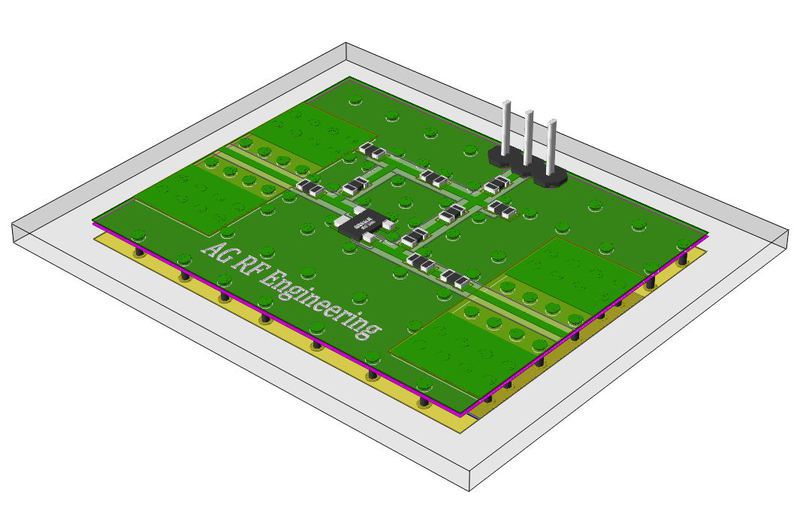 2.4GHz LNA Design
RF Layout is done for frequencies where wavelenght can be compared with size of a design structure the time delay, couplings and impedance mismatches can have significant influence on system performance. These are main properties to be controlled during the RF Layout design. Usually these are frequencies over 1 GHz, but can be also at the lower frequencies depending on systenm requirements.
These are main factors affecting the performance in layout:
- Parasitics of SMD components
- Parasitic capacitance to ground and impedance mismatches
- Grounding quality
- PCB to Device transimission effects
There are typical transmission line microwave structures used like baluns, couplers, isolators, microwave filters, etc. The layout can be realized in few different transmission line types like: Micro-Strip, Strip-Line, Suspended-Microstrip, Co-planar.
Technologies:
- PCB: FR4, Rogers, RT Duroid (typicaly after 20 GHz)
- Package: LTCC, HTCC, Leadframe
- Microwave: Coaxial, Waveguide, Microstrip, Stripline, Co-planar, Antennas
Applications:
- SAT TV, GPS, GSM, LTE, LTE=A, Radar, Digital radio, Digital TV
- ISM Band: WIFI, Bluetooth, etc.
Tools:
- AWR Microwave Office, Visual System Simulator
- Tina, Matlab, Eagle
- Other on request
We are offering High Frequency circuit layout design for PCB/LTCC devices and modules, as well as verification of existing designs, prediction of performance, tunung and optimization including system simulation.