
Services
CAM Library models
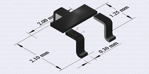
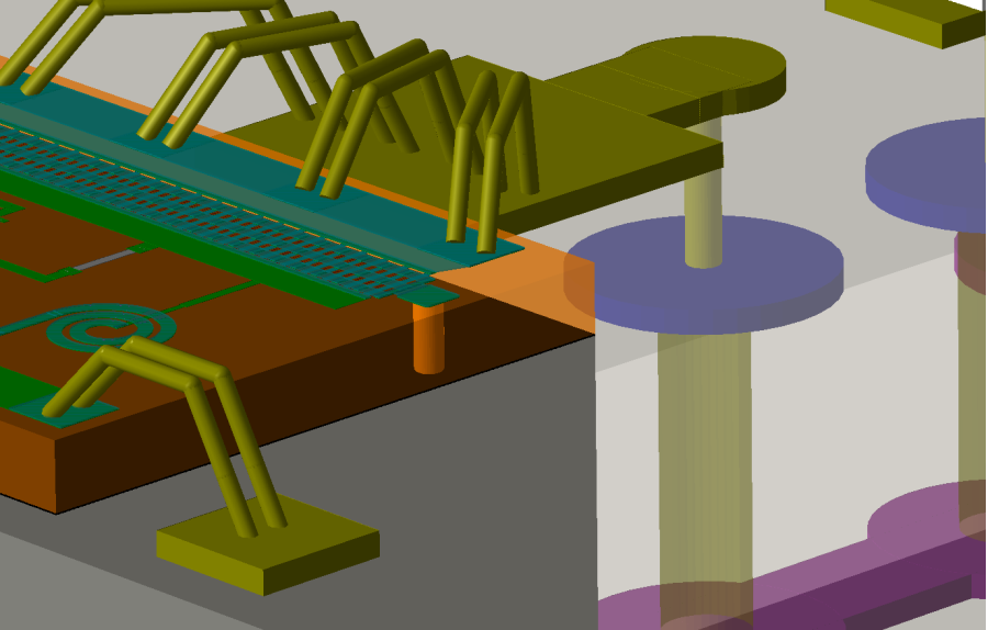
Your design starts from correct CAD models for design, simulation and manufacturing setups
Our EDA and CAD Model services:
- 3D CAD Models and 3D Prints
- EM-based SPICE models
- Touchstone models from measurements
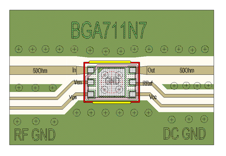
- RF Footprints and Layout blocks
- PCB Footprints (IPC norm)
- EDA component Libraries and Process libraries (PDK)
Customer benefits:
- High quality CAD and simulation models for any design system
- Fast design start with proper components
- Further support and verification services
Design Verification
 Design Verification
Test the fuctionality and robustness of your design before manufacturing and optimize it for high end performance.
Our verification services:
- RF System Verification on the System and Circuit Levels
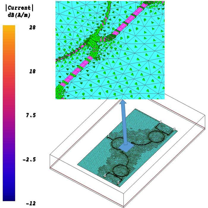
- 3D EM Simulation for RF and digital systems
- Antenna Simulation
- Thermal and Mechanical Verification
- Signal Integrity Analysis for High Speed Signals
- EMC Analysis
Customer advantages:
- You are coming ahead of your competitors due to shorter design cycle and time-to-market time
- Provide your customers optimal performance of your product
- Know the limits of your system
Software Solutions
Missing features in EDA and CAD tools braking down the development process. Add-Ins automate routine manual work and make design process faster and more efficient.
General productivity apps:
- Memo on Top - Picture-in-Picture tool for windows desktop
- XML File tagging - alternative to Microsoft Sharepoint technology
Apps for AWR MWO:
- Schematic: Components Search, Nets Annotation
- Layout: Fast layer manager, Auto-Ground
- CAM: BOM, P&P generation
- Interfaces: Gerber import, Eagle Comunicator, HFSS Export, other
- Signal Integrity Analysis Package: Net Annotation, Layout to Schematic Interconnect
Development of analog and digital wireless electronics according to the customer specification
Development of RF front-end electronics for telecommunication and sensors.
Customer benefits:
- Project planning and controlling
- Innovative development methods
- Orientation on customer requirements
- 15 years of RF experience
PDK Design
Process Design Kit (PDK) organizes development process including most common design data: Layout rules, components, Footprints, 3D Information, Manufacturing data, etc. What is extremely important for team work and minimizing of double effort.
PDKs available:
- RF PCB Process
- LTCC Design Process
- Laminate Design Process
- Leadframe Design/Simulation Process
- Provides full design flow including Schematic, Layout, Simulation Extraction and Production Automation
Customer benefits:
- Fast kick-off time of projects
- Strong automation of design processes
- Interoperability with CAM systems
- Easy sharing and team communication for technical topics
- Advanced design models