
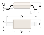
Footprints according to IPC Standard
(Land Patterns)

Footprints for your design process, depending on the technology (PCB, LTCC...). You can choose design rules (e.g. minimum metal pitch, solder mask pitch, etc.). Solder mask method – NSMD or SMD.
Our footprints include all needed layers for modern design including “center cross”, “keep out area”, “Solder Mask”, etc. It is possible to have special customer layers or special layer
names.
All dimensions are in accordance to IPC standard.
Sizes
- minimal footprint size (for compact designs)
- nominal footprint size
- maximal footprint size (good mechanical stability)
- user settings (for specific designs e.g. high frequency designs)
Layer list:
- Metal
- Solder Mask
- Solder Paste
- Component size - (Package)
- Silk Screen
- Keep Out Area - (Important for the right component clearance)
- Center Cross - (Important for the right automatic mounting)

It is also possible to use additional layers such as:
- Leads
- Documentation, etc.
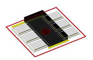
 Example for 2 Leads Package
Device Types
- SMD
- Through Hole
- Connectors
- Test Points
- Thermal Vias
- Other
Complexity
- Any Pin number
- DRC complains can be analyzed
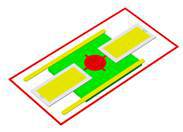
 Example for TH Connector
Available CAD/EDA Systems
- Altium Designer (earlier PCad)
- Cadence Allegro, OrCAD
- Eagle PCB
- AWR Microwave Office
- Mentor PADS
- Mentor Xpedition
- Zuken CADSTAR
- Zuken CR5000
- Dip Trace
Others (optional)

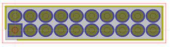
Example for BGA600 Package
We are working with the most of PCB, CAD and EM software as Eagle, Dip Trace, Altium, AWR Microwave Office, ADS and many others.
We can design any footprint type, size and any footprint difficulty.
For all the questions, please contact info@ag-rf-engineering.de