
AWR Process-Design-Kits design service
Process-Deisgn-Kits (PDK) for AWR MWO - single or mixed technology design setups forPCB, LTCC, HTCC, Laminate or Semiconductor.
Benefits of the PDKs
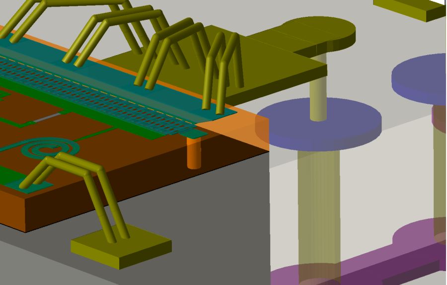
- Substrates, traces, via, bond-wires accord to the technology process and DRC
- iNets routing capability for layout
- Equivalent circuit and EM simulation extraction for electrical verification
- PCell libraries with parameteric layout and simulation data
- Standrd components libraries for design
- Enables top-down design flow from concept to Gerber or GDS generation
About AWR MWO
AWR MWO - is a leading tool in intelligent design of HF&mmWave MMIC and PCB design. AWR MWO uses leading EDA technologies to simplify and empower the HF design with unified schematic and layout data-base, modern simulation engines and simulation sockets to CST, HFSS and other simulators.
About the PDKs
PDK (Process Design Kit)
- is a way how to include all technology process in AWR MWO. It reduces the development time of circuit, simplifies development, simulation and production flows, makes standard design process for design and manufacturing. Enables design of complex circuits with automation in schematic, layout, simulation and verification.
Key technologies used in AWR PDKs
iNets - the routing technology, using intelligent nets to route traces between layers according to the design rules, extract traces into circuit simulator and analyse impedance, parasitics and cross-couplings in the circuit.
DRC - Design Rule Checker verifies complains between production process and layout design.
PCell - parameteric library cell. Incorporates the rules for the parametric layout drawing of the components (like coils, capacitances or transistors) for the used production technology and simulation data for the element. The simulation data is derived from the Spice simulation model or EM-simulated data.
Circuit Extraction and EM Simulation - are taking in accoung line impedance effects, parasitic couplings, predicts and gives possibility to optimize electrical performance of the layout.
LVS - (Layout versus schematic check) verification of the correspondance between schematic circuit and layout implementation. This procedure preserves electrical layout mistakes.
BOM - (Bill of Materials) list of components and materials required for assembly of the final device.
P&P - (Pick & Place) coordinates for SMD components and their orientation, required for automatic assembly. It's typically used for PCB, LTCC pr laminate models.
We have a big number of tools for AWR MWO - a tool for HF development. These tools increase productivity and bring new capabilities for AWR MWO users.
Request a PDK for your technology:
Our work-flow add-ons for AWR MWO:
- EM simulation and Spice extraction
- Auto-documentation for AWR project
- 3D Layout export for mechanical design
- SMD Footprints and components libraries
- AWR2WEB - web simulation portal based on AWR MWO
- S-parameter viewer